BUSINESS
Newflex's technology enables us to create a better world.
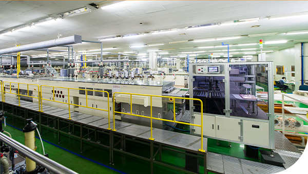
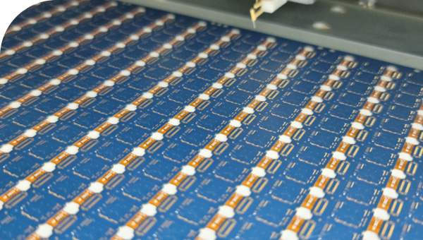
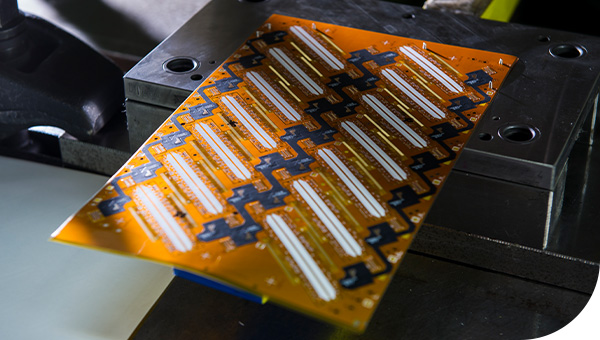
Production process
Each product is produced under strict management with a monthly production volume of MLB R.F: 40,000m2, Metal : 100,000m2
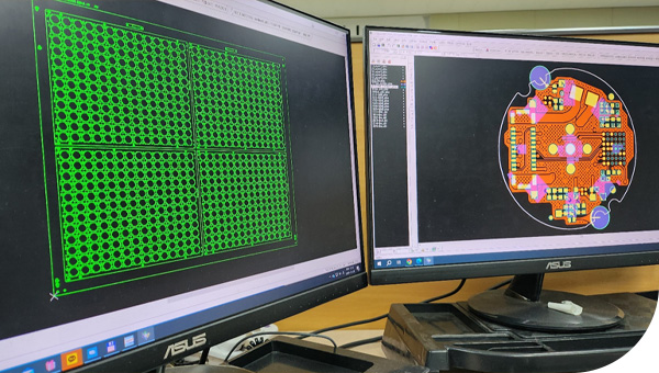
Artwork (CAM) 01
Process of real-time processing of the Artwork System and
Film Plotting for circuit design, modification, and panelizes
for the production process.
Film Plotting for circuit design, modification, and panelizes
for the production process.
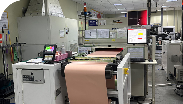
Drilling 02
Process of machining via holes and mechanism holes.
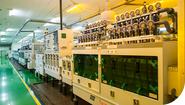
Copper Plating 03
Process of chemical copper and electric copper for
through-hole plating of double side & multi-layer products.
through-hole plating of double side & multi-layer products.
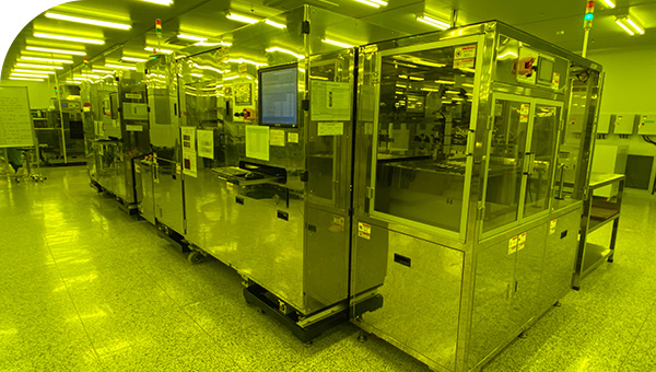
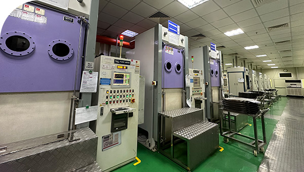
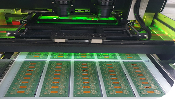
Imaging 04
Exposure process using an advanced imaging system
for circuit formation.
for circuit formation.
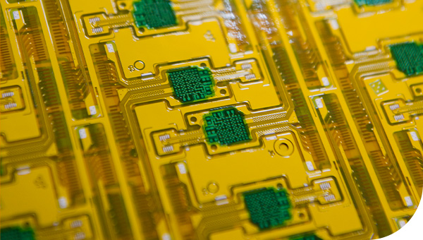
Etching & Wet Process 05
Process of forming a circuit using development, corrosion,
peeling, etc.
peeling, etc.
Coverlay Lamination 06
Process of laminating coverlay for solder resist.
PSR 07
Process of protecting the circuit formed area using
Photo Solder Resist Ink and opening the component mounting area.
Photo Solder Resist Ink and opening the component mounting area.
BBT 08
Process of electrically inspecting open/short circuits
and through holes.
and through holes.
Router & Press 09
Process of processing the external shape with router
and mold press, etc.
and mold press, etc.
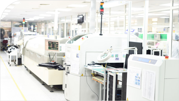
SMT 10
Process of mounting components such as capacitor/resistor
on FPCB.
on FPCB.
Final Inspection 11
Process of inspecting product appearance using
microscopes and inspection.
microscopes and inspection.
TEL : 031-494-9325 FAX : 031-493-1305
Copyright © 2023 NewFlex Technology Co., Ltd. All Rights Reserved.